
Catching up on a missed week here: Electronics design using Eagle, and getting a bit better at milling boards!
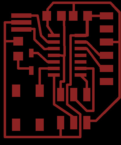
I found my .png out of Eagle had a lot of white space around it and perhaps as a result seemed to get resized to about 50% mwhen taken into Vcarve. I decided to do a workaround by scaling the image back to size in Vcarve, using a benchmark measurement off Loraine's Vcarve file. I later found that when I deleted the border line around the board in Eagle, the .png exported without all that free space. Hopefully this will solve the scaling problem for me in the future. Here is the corrected png:
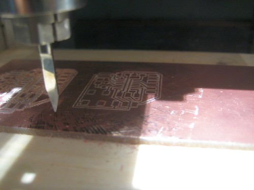
I tried a slightly different method of milling to previously - rather than pocketing, which took an awfully long time, we (Thom and I) decided to go for two profile paths, with the second offset by a tool's width to give a thick outline mill of all the traces. This proved a good method, and much quicker, along with a much increased feedrate of 10mm/s, using the same 20 degree engraving bit as before. We were now down to about 5 - 10 mins milling per board. For some reason the mill is still plunging at a much slower rate than I specify (0.5mm/s), so this time could be further reduced. I will need to investigate this further.
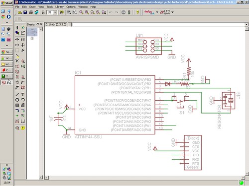
I then redrew my Schematic using the net labelling method described on the Providence tutorial here, having been shown that by Thom and Loraine. I quite liked my more messy rat's nest approach at the start but i can see the benefits of both! Here is the final schematic and board:

UPDATE
We got the 20Mhz resonators that we were missing, so finally got this board completed.

Basic design
Laying out the board was a fairly straight forward affair using the fab library provided, and the example image. I felt my way around Eagle and found it pretty easy to get to know, once you realise when adding a component from the library to click 'Ok' rather than 'Drop'! Another tricky bit of the interface was the 'change' button - took me a while to figure out that is how you edit trace widths.Milling
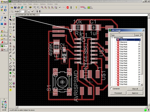
I was fairly pleased with my board layout when Joel pointed out the ERC and DRC buttons for checking the schematic electronically and the board for 'design rules'. I was keen to get milling however so started that process on the Modela and left exploring the ERC and DRC buttons to later.I found my .png out of Eagle had a lot of white space around it and perhaps as a result seemed to get resized to about 50% mwhen taken into Vcarve. I decided to do a workaround by scaling the image back to size in Vcarve, using a benchmark measurement off Loraine's Vcarve file. I later found that when I deleted the border line around the board in Eagle, the .png exported without all that free space. Hopefully this will solve the scaling problem for me in the future. Here is the corrected png:
Some Maintenance
Before I could mill, we had to clean our self centering vice which had become completely gunged up with swarf and cutting oil from some brass engraving another member had been doing recently. Stuart the lab technician patiently bathed the threads in WD40 and got things working smoothly again.I tried a slightly different method of milling to previously - rather than pocketing, which took an awfully long time, we (Thom and I) decided to go for two profile paths, with the second offset by a tool's width to give a thick outline mill of all the traces. This proved a good method, and much quicker, along with a much increased feedrate of 10mm/s, using the same 20 degree engraving bit as before. We were now down to about 5 - 10 mins milling per board. For some reason the mill is still plunging at a much slower rate than I specify (0.5mm/s), so this time could be further reduced. I will need to investigate this further.
Adjustments
My first attempt came out a good few millimetres too big, indicating that my manual scaling had been a bit off. I had mesaure between some adjacent pads, which meant that any error must have got scaled up over the board, so this time I measured over pads along the length of the board, giving a much more accurate result. I also found that 0.15mm was not deep enough to get through the copper in places so upped this to 0.25mm in selected bits of the board, and ran supplementary cutting paths for these. i also found that in some places my traces were very close so only the profile path with 0 offset allowance cut through - not ideal.Running ERC and DRC in Eagle
ERC threw up a couple of nets that apparently weren't actually connected, so I redrew them. DRC threw up a couple of places where I had realised in milling traces were too close - would have saved a good bit of time if I'd done that first!I then redrew my Schematic using the net labelling method described on the Providence tutorial here, having been shown that by Thom and Loraine. I quite liked my more messy rat's nest approach at the start but i can see the benefits of both! Here is the final schematic and board:
Populating
I am still waiting for some components to populate this board so will update as to its ultimate success or not as the case may be later!UPDATE
We got the 20Mhz resonators that we were missing, so finally got this board completed.


No comments:
Post a Comment